Samsung’s 2nd-gen 3nm direction of anticipated to enter prototype manufacturing quickly
Serving the tech enthusiast neighborhood for over 25 years.
TechSpot design tech prognosis and suggestion you can trust. Read our ethics assertion.
Rumor mill: If the rumors are correct, Samsung is heading within the genuine direction to meet its mentioned aim of initiating mass manufacturing of SF3 within the 2nd half of of this year. It’ll exercise the node to kind unusual product kinds and enhance performance on the Galaxy Peek 7 later this year.
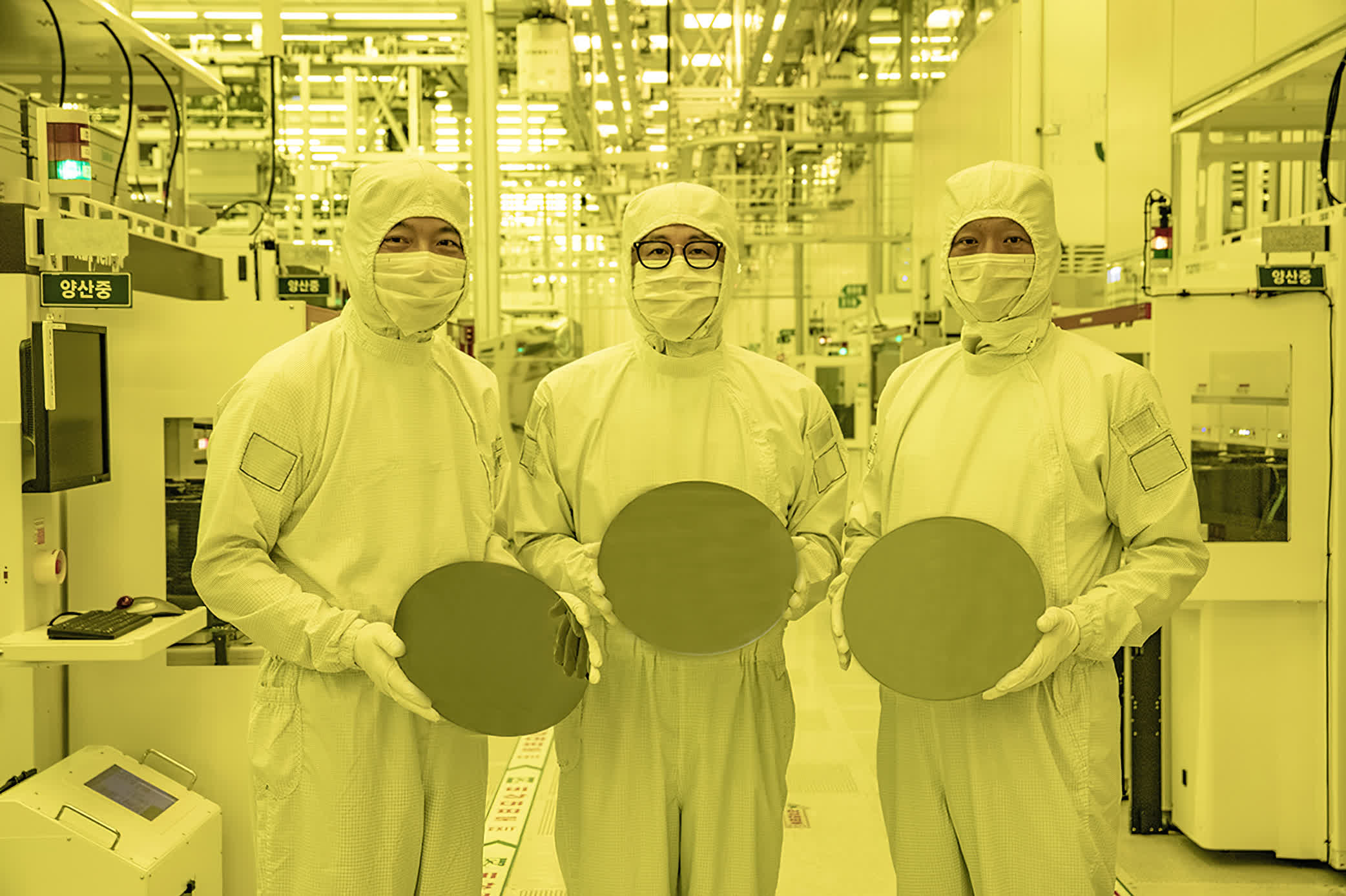
Slack remaining year Samsung announced it would commence mass manufacturing of its 2nd generational 3nm direction of, every so recurrently called SF3, as properly because the 4th generation 4nm direction of for HPC within the 2nd half of of 2024. Once performed, that could be a fundamental milestone for the firm as this could well enable it to kind unusual product kinds.
It looks that Samsung is heading within the genuine direction to meet this timeline. Unnamed industry sources find suggested Chosun that Samsung Electronics has begun manufacturing of prototypes the exercise of the 2nd-generation 3nm direction of and is within the mean time finding out the chip’s performance and reliability. It is concentrated on a yield of over 60 p.c for the 3nm 2nd-generation direction of for the length of the subsequent six months.
Samsung started mass manufacturing of its SF3E, or 3nm gate-all-round early, manufacturing technology in 2022 with special nanosheets that widen channels to encompass improvements in PPA, or vitality, performance and home. SF3 will exercise the firm’s 2nd-gen Multi-Bridge-Channel enviornment-cessation transistors (MBCFET), which is unusual fabrication technology that builds upon SF3E and introduces further optimization. In contrast with SF4, SF3 has a 22 p.c increased performance on the an identical vitality and transistor count, a 34 p.c vitality reduction on the an identical clocks and complexity, and a 0.79x good judgment home reduction. Briefly, SF3 could be higher suited for complex designs than the SF3E.
The upcoming Galaxy Peek 7, which is scheduled for liberate later this year, will find the first chip made on the SF3 node and is anticipated to be an application processor designed for wearables. The Galaxy Peek 7 will again as a test mattress and assuming all goes properly, Samsung will implement SF3 into Samsung Electronics Arrangement LSI’s Exynos 2500 for the impending Galaxy S25, which is anticipated to roll out subsequent year.

Other rumors give a enhance to the concept that the Galaxy Peek 7 could be fundamental for Samsung.
According to tipster Roland Quandt, the Galaxy Peek 7 will exercise an Exynos processor that is primarily based mostly on the Exynos 5535. It is that which that possibilities are you’ll maybe imagine that the chipset can also very properly be named the Exynos W940 – an enhance from the Exynos W930 that powered the 2023 watches. If these reports are correct, battery existence – quiet a effort level for smartwatches – must be vastly improved within the Galaxy Peek 7 when compared with the Peek 6.